This blog compares a traditional Vector Network Analyzer (VNA), the HP 8753, with a NanoVNA for use by the budget constrained engineer developing a medical device.
A Vector Network Analyzer or VNA injects a known signal into a circuit, and determines what changed about the signal after it leaves the circuit. VNAs are used during the development process of a device, to characterise and verify the performance of circuits such as amplifiers, filters, antennae, cables, etc. This is very common, especially if a given device operates at higher frequencies, where nonidealities can play a bigger role and are harder to predict.
VNAs exist in many sizes, shapes, and price ranges, all with varying features and capabilities. Two examples of VNAs are the NanoVNA-H, and the HP 8753. The NanoVNA-H is an affordable hand-held amateur VNA, and the HP 8753 is a trusty professional labs workhorse of the 90’s. The market and intended use case of the HP 8753 and NanoVNA-H are fundamentally different. The wide range of equipment available for sale raises many questions, such as whether or not low-cost versions have a place in a professional engineering environment.
Later in this blog I will measure the frequency response of four fundamental filter topologies from a sample PCB on both VNAs.
Initial comparison of NanoVNA-H and HP 8753
Upon first look at these devices side by side, it would be fair to think they did vastly different things. Despite almost comical physical differences, these devices are designed to do almost the same task.
| NanoVNA-H | HP 8753 | |
| Accuracy | 0.5ppm | 10ppm @ 25C |
| Resolution | ? | 1Hz |
| Frequency range | 50khz to 1.5Ghz | 30Khz to 3Ghz |
| Dynamic range | 70dB (50kHz-300MHz), 50dB (300-900MHz) and 40dB (900-1500MHz) | 110dB (30kHz-3GHz) |
| Price range | $50-$200 (new) | $3000-$8000 (used) |
Comparing specifications of a device produced by one of the highest end instrumentation companies for decades with an open-source device can be tricky. The specifications listed for the Nano VNA-H are likely not completely accurate and I was unable to find a reliable source for the resolution. It’s also worth noting the frequency range of the NanoVNA can get up past 1.5Ghz with a firmware update, however the accuracy and resolution goes down dramatically with this modification. Furthermore, you can see that the dynamic range of the NanoVNA-H drops quickly as frequency increases, due to it needing to down convert frequencies greater than 300Mhz as its receiver cannot directly measure anything above this frequency.
The NanoVNA-H’s accuracy spec is quite impressive and appears to have been verified by amateur radio operators but, to my knowledge, has not been verified through a NIST chain. As the NanoVNA and HP 8753 are from different eras of design, it is important to discuss the context around why these instruments exist. The NanoVNA is an open-source project, first released in 2019, intended for hobbyist electronic circuit design and testing. It is quite popular in the amateur radio community and is a staple on the desk of many HAM operators and tinkerers.
This contrasts the HP 8753, which was developed in the late 1980s, intended for use in professional settings to be used day in and day out by engineers designing various forms of electronic devices. Many of the technologies and components used in the design of the NanoVNA were merely ideas in the 1980s. The development of each instrument reflects the time it was developed in.
Advantages of NanoVNA
The NanoVNA comes equipped with many newer communication standards, such as a microSD card, and a USB-C port for charging and connection to a desktop control environment. This could be useful for running automated tests, collecting large amounts of data or changing settings without needing to use the small touch screen. It is also much smaller (weight/volume) making it very appealing for portable applications, especially with the integrated battery.
As it is open source, the NanoVNA could be a very appealing launch pad for the development of medical devices that have a similar mode of operation, or as a tool for an engineer looking to expand their high frequency circuit design expertise. This makes the approachable price tag of $50-200 CAD (depending on supplier) very appealing for engineers of varying levels of experience, especially when working on budget sensitive applications. It is also capable of being calibrated by the end user via the SLOT method; utilising short, open, load and termination connectors and cables. This is very simple and can be performed in a manner of minutes. If your cable and termination plugs’ characteristics are trusted, you can have some faith that your waveforms are close to representative of what you are measuring. Lastly, the NanoVNA uses SMA connectors, which are very cheap and commonly available.
Disadvantages of NanoVNA
The biggest disadvantage to its open-source nature is many illegitimate clones exist for sale with various levels of quality and capability. Furthermore, there is not a lot of information available for the accuracy/repeatability over its frequency range, which can be a major detractor for sensitive applications. While this device can be calibrated by the end user, changing the frequency span of the display requires recalibration, which could be a hassle if done repeatedly. Furthermore, the NanoVNA is only capable of directly measuring S11, S21. All other parameters are calculated from these two measured values, which could introduce some inaccuracy.
Advantages of HP 8753
The biggest advantage of the HP 8753 is its frequency range, from 30khz to 3ghz. It has numerous features the NanoVNA does not, such as 4 port measurement. There are two aspects that the HP 8753 wins out over any open source VNA: maintenance and calibration. While the HP 8753 was originally manufactured by HP in the very late 80s, Keysight (a spin-off of HP’s instrument division) still offers repair/maintenance for it, which can be a big benefit for companies without in-house repair capabilities. This is evidently not the case for the nanoVNA, as you are on your own if something is damaged.
Furthermore, the HP 8753 can still be professionally calibrated. This is a key advantage, especially in the medical device field as ISO 13485 requires equipment to be calibrated when used for verification and validation. While the HP 8753 is not open source, schematics exist in the service manuals for the entire device and can be found online. This is also great for learning about high frequency schematic design, albeit from a very different era of circuit design.
Disadvantages of HP 8753
Unsurprisingly, most of the detractors for the HP 8753 are due to its age and cost. It is bulky, weighing in at 34 kilos, making it less than ideal for portable applications. Due to its age, the screen is dim, making reading it a challenge. It lacks more modern communication interfaces, with our model only being equipped with a floppy drive and HPIB. This can be frustrating when you are trying to get multiple high-quality plots off the instrument for reports, presentations etc. Furthermore, the HP 8753 uses type-N coaxial RF connectors, which can be quite expensive compared to BNC connectors or the SMA connection present on the NanoVNA.
Real-life testing
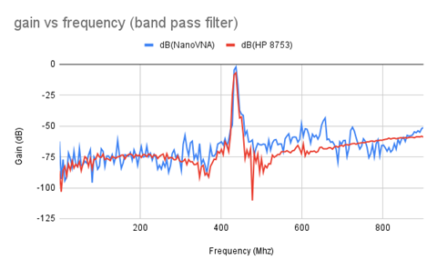
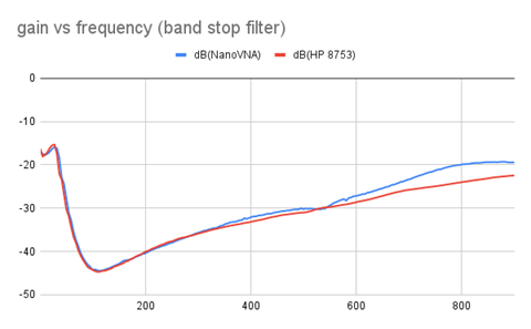
To get a sense of how these instruments compare in real-life, I measured four filters on a sample PCBA: A band pass, band stop, high and low pass filter. These filters were chosen due to their ubiquity, however there are many other advanced circuits the VNA can analyze.


After generating and viewing these graphs, I was quite pleased to see that the data coming off both the HP 8753 and NanoVNA was very similar. Some differences could be explained by factors such as time since calibration for the HP, and connector/cable nonidealities for both instruments. In general, I think the data coming out of both devices could be used for specific points in the development process without any issue.
Conclusion
Unsurprisingly, the answer to the question I posed at the beginning of this blog is not as straightforward as it might seem. If you spend most of your time at a desk or bench performing verification of electronic circuits, a trusted device like the HP is an appealing option. If you are an engineer at a start-up where funds for expensive instruments might not be available, or you are doing design work that will later be verified by higher-end instruments, I would seriously consider an open-source device like NanoVNA. No matter which option you choose to use, a person new to high-frequency design will benefit from using these devices to understand high frequency circuit behaviour that is not obvious in everyday circuits, and from perusing the schematics and flow charts made available by both manufacturers.
Images: StarFish Medical
Mike Ganzert is an Electronics Engineer at Starfish Medical. He received his Bachelor’s of Applied Science in Electrical Engineering from UBC Okanagan in 2021, with a focus in medical devices.


